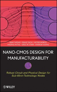
Nano-CMOS Design for Manufacturability
Ban P. Wong, Andrew Kahng, Greg W. Starr, et al.
* Affiliatelinks/Werbelinks
Links auf reinlesen.de sind sogenannte Affiliate-Links. Wenn du auf so einen Affiliate-Link klickst und über diesen Link einkaufst, bekommt reinlesen.de von dem betreffenden Online-Shop oder Anbieter eine Provision. Für dich verändert sich der Preis nicht.
Naturwissenschaften, Medizin, Informatik, Technik / Elektronik, Elektrotechnik, Nachrichtentechnik
Beschreibung
Discover innovative tools that pave the way from circuit and physical design to fabrication processing Nano-CMOS Design for Manufacturability examines the challenges that design engineers face in the nano-scaled era, such as exacerbated effects and the proven design for manufacturability (DFM) methodology in the midst of increasing variability and design process interactions. In addition to discussing the difficulties brought on by the continued dimensional scaling in conformance with Moore's law, the authors also tackle complex issues in the design process to overcome the difficulties, including the use of a functional first silicon to support a predictable product ramp. Moreover, they introduce several emerging concepts, including stress proximity effects, contour-based extraction, and design process interactions. This book is the sequel to Nano-CMOS Circuit and Physical Design, taking design to technology nodes beyond 65nm geometries. It is divided into three parts: * Part One, Newly Exacerbated Effects, introduces the newly exacerbated effects that require designers' attention, beginning with a discussion of the lithography aspects of DFM, followed by the impact of layout on transistor performance * Part Two, Design Solutions, examines how to mitigate the impact of process effects, discussing the methodology needed to make sub-wavelength patterning technology work in manufacturing, as well as design solutions to deal with signal, power integrity, WELL, stress proximity effects, and process variability * Part Three, The Road to DFM, describes new tools needed to support DFM efforts, including an auto-correction tool capable of fixing the layout of cells with multiple optimization goals, followed by a look ahead into the future of DFM Throughout the book, real-world examples simplify complex concepts, helping readers see how they can successfully handle projects on Nano-CMOS nodes. It provides a bridge that allows engineers to go from physical and circuit design to fabrication processing and, in short, make designs that are not only functional, but that also meet power and performance goals within the design schedule.
Kundenbewertungen
Schaltungsentwurf, Electrical & Electronics Engineering, Circuit Theory & Design, Schaltkreise - Theorie u. Entwurf, Nanotechnologie, MEMS, Elektrotechnik u. Elektronik, Nanomaterials, Nanotechnology, Nanomaterialien
